We are happy to receive students from Physics, Chemistry, Nanotechnology, Mathematics, and many other education programs with which we have extensive experience, so do contact us at “cops@utwente.nl“.
Projects can often be tailored to either BSc or MSc phases, please contact us with your study requirements. Since Nanophotonics is a dynamic field, topics in fashion may change rapidly, so contact us to hear the latest. And if you have your own project proposition: you are most welcome to come to discuss it. Our labs are in the Meander building of the UT, where we are proud of making the best coffee on campus! Projects below:
A PowerPoint presentation containing projects by COPS to participate in the Saxion International Student Week.
240204_SAXION International Project Week 2024
****************************************
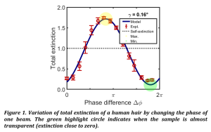
Mutual extinction: Making human hair transparent
In this BSc project, we want use and expand an existing setup [2] to perform mutual extinction measurements to make a scattering sample (e.g. a human hair) transparent. Additionally, we can use an automatic rotating arm to extract the true phase difference between the laser beams to further characterize the scattering sample.
This project will partially involve design, experiments, and analysis. If you have any questions or are interested, see this flyer (NA_2025_project_mutual_extinction) and/or send a mail to n.f.l.alferink@utwente.nl.
****************************************
An important step to the realisation of optical computers is the storage of photons. One way of storing photons is by trapping them in an extremely disordered material, the photons keeps bouncing around and cannot leave! This phenomenon is called Anderson localisation of light. Unfortunately, no one has been able to show that this also happens in real, three-dimensional materials.
In this MSc project you will build your own optical setup to measure the reflection and transmission properties of highly advanced nanophotonic samples. There is a lot of space for creativity with a clear goal ahead. If you have any questions or are interested, see this flyer and/or send a mail to l.mulder-1@utwente.nl.
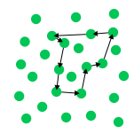
Figure 1. Due to the extremely strong light scattering the photon will keep bouncing around and is thus trapped.
****************************************
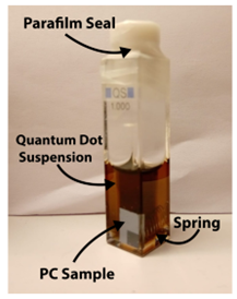
At COPS, large 2D photonic crystals are fabricated by etching 5 μm deep pores in a silicon wafer. The goal of this project is to probe the local DOS (LDOS) inside the photonic crystals by measuring the radiative decay rate of quantum dots inside the structures. That way, we better understand the optical properties of these photonic crystals.
The project is engaging in many different ways. To name a few of the challenges you will encounter: (A) Quantum dots oxidize quickly when they are in contact with air, so filling the cuvette with quantum dots has to be done in a glove box. (B) There should be little to no space between the crystal and the cuvette wall, as we only want to measure emission out of the pores, and not outside. We have to measure the distance between the wafer and the cuvette wall and make sure it is much less than the pore depth (which was only 5 μm!). (C) Explaining experimental results using photonic crystal theory.
The image below (by previous student Pieter van Essen) shows a 2D photonic crystal etched on a large silicon wafer, held inside a cuvette with toluene and quantum dots. For more details about this project, see this flyer, or contact t.j.vreman@utwente.nl.
****************************************
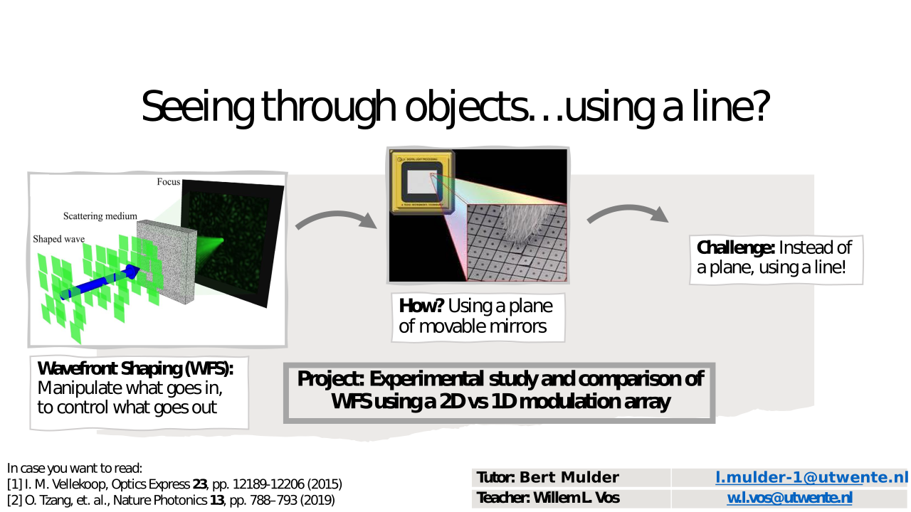
Wavefront Shaping (WFS) is a promising modern technique to improve microscopy (invented by COPS!) In WFS, we control the phase and amplitude of the incident wavefront to focus wherever we want, even inside the sample! Currently, our modulation is based on a 2D array of tiny movable mirrors. The question for this project is, can we exert sufficient control if we use a 1D array of mirrors (a single line) for WFS? And employ the other dimension for other control (e.g. color)?
For more information, contact Bert Mulder at l.mulder-1@utwente.nl
****************************************
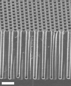
Bachelor project. The goal of this project is to measure and simulate the reflectivity as a function of frequency off a 2D photonic crystal etched on a large silicon wafer where the interface between the air and the photonic crystal is varied in a controlled way. An SEM image of the photonic crystal is shown below, where the scale bar is 1 micrometer. A more detailed description of this project can be found in this flyer, or contact t.j.vreman@utwente.nl.
****************************************
In most nanophotonic devices, embedded quantum emitters like quantum dots are excited by an external light source such as a laser. However, it would be “cool/hot/exciting” if quantum emitters could be excited & addressed electrically. Moreover, it allows to interface with the whole big world of CMOS, and silicon nanofabrication. Consider this: you could send single photons at the nanoscale with your phone! 🙂
This is an interdisciplinary project together with the HMOE and NBP chairs, see this flyer
Interested? Do contact Willem Vos (w.l.vos@utwente.nl), Chris Nijhuis and Christian Blum.
****************************************
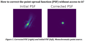
How to sharpen wavefront shaping by itself?
In this project, we will perform studies with an existing setup, adding a way to calibrate and correct aberrations for a non-trivial broadband source. Hence we will use a SLM. This will involve research, design, and programming. After improving the setup, we will be able to better illuminate and sharply image 3D Photonic Band-Gap Crystals Superlattices!
If you are interested or want more information, please consult this flyer, and/or contact m.e.l.hubert@utwente.nl
****************************************
You can find more information of the projects in the links below
| 2020 COPS projects for BSc/MSc students | ||
|
||