How to make light flat and send it backwards? Stick it on a 3D photonic band gap!

An intriguing kind of light control is the opportunity to have photons propagate preferentially in a thin quasi-two-dimensional (2D) sheet in space, where propagation in the third dimension is exponentially attenuated or otherwise somehow impeded. Such peculiar “flattened” light propagation is well known on a single interface between a metal (with negative ɛ′m < 0) and a dielectric (with ɛ′d > 0), where surface plasmon polaritons occur (also on their double-interfaced counterparts). A second way to flatten light occurs on the surface of a 3D photonic band-gap crystal, where surface states occur that have been observed in pioneering studies by Ishizaki et al from Kyoto. A third approach is to confine light to a thin single-mode waveguide formed by a line defect in a 2D slab photonic crystal, such as the famous W1 waveguide. In these platforms, light has wave vectors exceeding those in free space (“outside the light cone”), hence special in or outcoupling methods are needed to overcome the momentum mismatch, such as gratings or prisms.
Recently, COPS scientists Timon Vreman and co-workers have discovered yet another way to flatten light! They fabricated a silicon nanostructure to confine light to a thin 2D layer: a layer that acts as a surface defect on a 3D photonic band gap crystal. When a 3D photonic band gap is (boldly!) considered as an effective medium, it appears to have a negative epsilon just like a metal. But the “fun” of a 3D band gap is that it is accompanied with zero absorption, as opposed to metals.
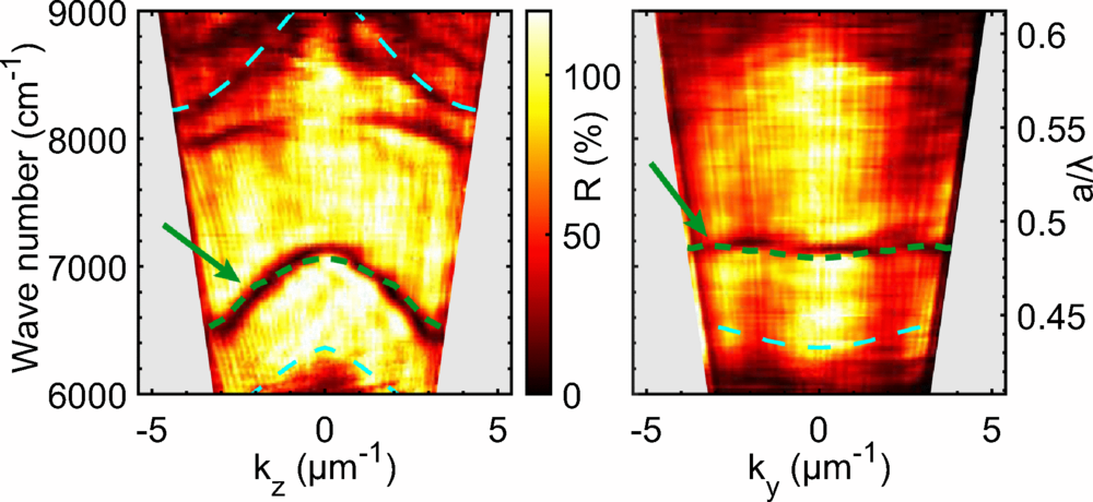
In their experiments the team observed that the confined waves are excited with a remarkably high efficiency (90%). Strikingly, the waves are found to run in a backward direction (see image), due to the periodic nature of the surface defect. Reflectivity experiments agree well with theory (supercell calculations) and with finite-difference time-domain simulations. The results further demonstrate the power of nanomaterials to control light. As an application, Vreman et al foresee a sensing device where the direction of photons emitted by embedded quantum emitters (e.g. quantum dots) is sensitively determined by the emission frequency.
The Team
The research was done by Timon Vreman, Melissa Goodwin, Lars Corbijn van Willenswaard, Bill Barnes, Ad Lagendijk, and Willem Vos from the University of Twente.
The paper
The paper entitled “Dispersion of backward-propagating waves in a surface defect on a three-dimensional photonic band-gap crystal” has appeared as “open access” in Physical Review B that is published by the American Physical Society (APS). The paper is available online or on the COPS website.