How to turn ultrathin silicon black?

Silicon is the basic material that is used in our smart phones, in optical sensors, or in solar cells on our roofs. It is a major outstanding challenge that silicon absorbs incident light only weakly, especially in the red part of the visible spectrum. Recently, using extensive computations, COPS scientists have discovered that a 3D nanostructured back reflector greatly increases the absorption. The back reflector is also made of silicon which is convenient to integrate with ultrathin silicon films. Consequently, next generation devices can be made ultrathin, which allows new devices to be much more flexible and compact. The results appear in the leading journal Optics Express that is published by the Optica society (formerly the Optical Society, OSA).
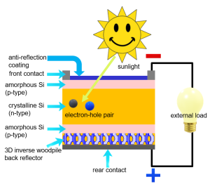 Figure 1: Example of a thin photovoltaic cell where the absorption of light is increased thanks to a 3D nanostructured back reflector – a 3D photonic band gap crystal – that thoroughly recycles unabsorbed light. Hence, an ultrathin photovoltaic cell could harvest much more light (than a cell without such a back reflector) to power an appliance such as lighting.
When incident light is absorbed by a plate semiconducting material like silicon, negatively charged electrons are excited from the lower-energy valence band to the higher-energy conduction band and similar for positively charged holes (that represent the lack of electrons). By attaching electrodes to the plate, the electrons and holes are harvested and sent into an electric circuit to drive a useful appliance. This process notably occurs inside a solar cell, see Figure 1, where the harvested current serves to power an LED for ambient lighting.
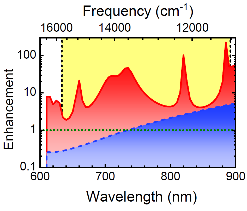
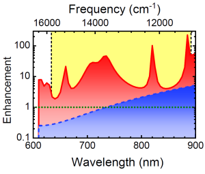 Figure 2: Absorption enhancement (ratio of absorption with a back reflector and absorption without back reflector) for an 80 nm ultrathin silicon layer. The red curve pertains to the ultrathin film with a 3D photonic band gap back reflector. The blue dashed curve pertains to an ultrathin film with a, hypothetical, perfect metal back reflector. The green line indicates the reference level (= 1) of the ultrathin film without any back reflector.
While thick silicon plates are widely used, thin silicon films are enjoying a rising popularity on account of their obvious sustainability, since they require much less material, less resources, and lower cost. Unfortunately, however, thin and ultrathin silicon films hardly absorb light, especially at long wavelengths in the visible spectrum where the sun radiates a lot. In other words, thin silicon films are not “black”. Therefore the team set out to study how a back reflector could recycle unabsorbed light, and become highly absorbing, or “black”.
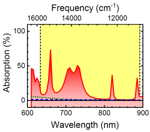 Figure 3: Absolute absorption (in %) for an 80 nm ultrathin silicon layer. The red curve pertains to the ultrathin film with a 3D photonic band gap back reflector and the blue dashed curve pertains to a perfect metal back reflector. The green line shows the absorption of an ultrathin film without any back reflector.
As a back reflector, the Twente team studied a diamond-like photonic crystal composed of two sets of perpendicular pores, shown in Figure 1. Such photonic crystals are known to have a record-wide 3D photonic band gap. As a result, the team indeed finds that this crystal is a truly omnidirectional, broadband, and polarization-robust back reflector. Lead author Devashish effuses: “Our extensive computations reveal that the photonic back reflector yields a striking 9.15 times enhanced absorption even for a 80 nanometer ultrathin film (see Figure 2). Our devices are up to 80% lighter than bulk silicon, due to the porosity of the photonic structure, jokingly referred to as “holeyness””.
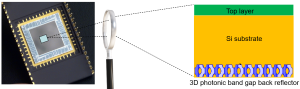 Figure 4: Schematic of a thin charge-coupled device (CCD) whose absorption could also enhanced by a 3D photonic band gap back reflector. Hence, such a CCD becomes more efficient at collecting light, and hence your holiday snaps.
Group leader Vos explains: “Such a strong absorption in a thin silicon film (see Figure 3) can also be interpreted in a quantum physical picture, namely that the photonic crystal acts as a colored electromagnetic vacuum below the absorbing film. The absorption of incident light is so strongly boosted that ultrathin silicon would effectively turn black”. The Twente team also projects that their holey 3D inverse woodpile structures offer application potential for compact on-chip sensors, photodiodes, and charge-coupled devices (CCD) for cameras (see Figure 4).
Previously, the team reported enhanced optical absorption for realistic and finite 3D silicon photonic band gap crystals with an embedded resonant cavity (https://nano-cops.com/publications/article/three-dimensional-photonic-band-gap-cavity-with-finite-support-enhanced-energy-density-and-optical-absorption/). The absorption was found to be substantially enhanced, however, only within the tiny cavity volume as opposed to the present case, where the absorption occurs throughout the whole film.
Information not for publication
The team:
The research was performed by Drs. Devashish Sharma, Shakeeb Hasan, and Rebecca Saive, and Profs. Jaap van der Vegt, and Willem Vos from the Complex Photonic Systems (COPS) chair, and the Mathematics of Computational Science (MACS) chair, both part of the MESA+ Institute for Nanotechnology, at the University of Twente, The Netherlands. Meanwhile, Sharma and Hasan joined ASML, the world-leading lithography company in Veldhoven, and Saive has become Associate Professor in the Inorganic Materials Science (IMS) chair at the University of Twente.
Funding:
The research was supported by the Shell-NWO/FOM Program ”Computational Sciences for Energy Research” (CSER), NWO-FOM program nr. 138 “Stirring of light!,” NWO-TTW Perspectief program P15-36 “Free-form scattering optics” (FFSO), NWO ENW-GROOT program (OCENW.GROOT.2019.071) “Self-assembled icosahedral photonic quasicrystals with a band gap for visible light”, the “Descartes-Huygens” prize of the French Academy of Sciences to WLV, and the MESA+ Institute section Applied Nanophotonics (ANP).
Paper on the web:
The paper has appeared online in Optics Express, volume 29, Issue 25, pages 41023 to 41047 in November 2021 (open access at https://www.osapublishing.org/oe/fulltext.cfm?uri=oe-29-25-41023&id=465409.) A copy of the paper is freely available on the COPS website at https://nano-cops.com/publications/article/enhanced-absorption-in-thin-silicon-films-by-3d-photonic-band-gap-back-reflectors-for-photovoltaics. It is also available on the Cornell preprint server Arxiv at: https://arxiv.org/abs/2106.15851
Contact for more info:
Dr. Devashish Sharma, email: d.devashish-1@utwente.nl, phone: +31 (0)6 16322202,
Prof. Willem Vos, email: w.l.vos@utwente.nl, phone: +31 (0)53 489 5309 (secretariat), +31 (0)53 489 5388, or +31 (0)6 47386517 (mobile).