Looking inside 3D nanostructures without leaving a trace

Discovering what is inside a three-dimensional (3D) nanostructure is no longer a matter of cutting it in slices, thus breaking it up and destroying its functionality. Scientists from the University of Twente and the European Synchrotron Radiation Facility (ESRF) discovered a new non-destructive method to look deep inside a 3D nanostructure. This ‘traceless X-ray tomography’ (TXT) can be applied to photonics, electronic chips, and computer memories, for example. The results are published in the magazine ACS Nano of the American Chemical Society.
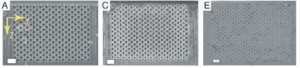 Fig. 1: Electron microscope images of three 3D photonic crystal nanostructures fabricated in the same way. Each external surface looks closely matches the design and looks like the other, but the functionality and internal structure will appear to be completely different.
Today, nanostructures are complicated 3D ‘buildings’, for example, to manipulate light (Fig. 1). Silicon electronics chips, as well, consist of multiple layers of material and interconnecting wires. But how do architects know if the full 3D nanostructure matches their expectations? By looking through a microscope, only the external surface can be checked. At this surface level, a ‘good’, a ‘bad’, or an ‘ugly’ sample may look perfectly the same. One way to look deeper inside is to cut the nanostructure in thin slices and examining those, one by one. Obviously, the nanostructure then loses its functionality. The new techniques also creates slices, but these are 2D images, not physical slices, that together form a 3D image. The nanostructure is still fully functional after the inspection.
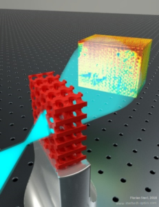
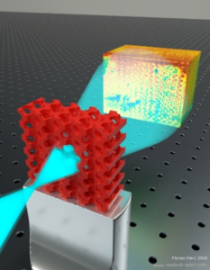
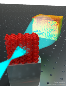 Fig. 2. Animation sequence showing that TXT data are recorded while rotating the sample (three orientations are shown). From the recorded radiographs, the tomographic reconstruction is derived that is shown in the background.
Thicker than one millimeter
Although X-ray technology has been used for a long time, it is often still necessary to cut a sample open in order to reach sufficient depth and contrast. The new traceless X-ray tomography (TXT) takes advantage of a high X-ray photon energy, thus making it possible to look into samples that have a silicon thickness of over 1 millimeter. First author of the ACS Nano paper Dr. Diana Grishina (now at ASML) explains: “This is up to 20 times thicker than with existing tools! In modern nanotechnology this is sufficiently thick to image through whole wafers. Indeed, all silicon devices remained untouched and ‘as is’ during our study.” The new method also makes it possible to zoom-in on a desired region.
Higher photon energy
In the experiment, the X-ray beam with a photon energy of 17 kilo electron volt (keV) is focused to a tiny spot of 23 nanometer by 37 nanometer. These holographic tomography experiments were done at the European Synchrotron Radiation Facility (ESRF) in Grenoble, France. Cloetens: “The sample is moved and rotated to create an image at each depth. In the end, intensive processing is done to combine all separate image slices in one complete 3D image.”
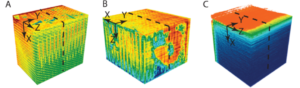 Fig. 3. Birds-eye view of reconstructed 3D silicon nanostructures shown in the SEM images in Fig. 1. (A) 3D photonic crystal that reveals a broad photonic gap in agreement with theory: “the Good”. (B) 3D photonic crystal that reveals a large void due to stiction resulting from violent liquid evaporation in the pores: “the Bad”. (C) Sample that shows shallow pores due to a fabrication error: “the Ugly”. The nicknames are inspired by a famous “spaghetti western” (link).
The Good, the Bad, the Ugly
As an example, the researchers studied so-called photonic bandgap crystals, a recently developed breakthrough in nanophotonics to completely control light. Its functionality depends on many deep pores in two directions, creating a prison in which light is manipulated. Although at the surface the nanostructures seem identical, looking inside revealed that one set of samples matches the designed structure, hence they were called ‘the Good’. Another sample had a large void inside since an infiltrated liquid had evaporated rather violently, hence it was called ‘the Bad’. A third sample revealed only shallow pores due to a manufacturing error and was thus called ‘the Ugly’. Leader of the Twente team Prof. Willem Vos: “When your sample performs different than expected, TXT non-destructively differentiates why you find a different structure or different performance. You can then still use the sample or study it further. This is why TXT is an original and powerful tool to critically assess 3D functional nanostructures.”
The research was done in the Complex Photonic Systems (COPS) chair of UT’s MESA+ Institute, in close collaboration with Dr. Peter Cloetens’ team at the European Synchrotron Radiation Facility in Grenoble (ESRF), France. It was made possible by the NWO programme ‘Stirring of Light!’, the Shell/NWO programme ‘Computational Sciences for Energy research’, the Descartes-Huygens Prize of the French Academy of Sciences, and contributions of MESA+ (Applied Nano Photonics) and the ESRF (beamtime grants).
The paper ‘X-Ray Imaging of Functional Three-Dimensional Nanostructures on Massive Substrates’, by Diana Grishina, Cornelis Harteveld, Alexandra Pacureanu, D. Devashish, Ad Lagendijk, Peter Cloetens and Willem Vos, is being published in the journal ACS Nano published by the American Chemical Society (ACS). A pdf of the paper is freely available on the ACS Nano website: https://doi.org/10.1021/acsnano.9b05519 or here on the COPS website, where you will also find many animations!
The Team
The research was performed by Dr. Diana Grishina, Cornelis Harteveld, Dr. Devashish, Prof. Ad Lagendijk, and Prof. Willem Vos from the Complex Photonic Systems (COPS) chair of the MESA+ Institute for Nanotechnology at the University of Twente, The Netherlands, and by Dr. Alexandra Pacureanu and Dr. Peter Cloetens of the European Synchrotron Radiation Facility (ESRF) in Grenoble, France. Meanwhile Grishina and Devashish have joined ASML the world-leading lithography company, and Pacureanu joined University College London (UK).
Support
The research project was supported by by the “Stirring of light!” program of the “Nederlandse Organisatie voor Wetenschappelijk Onderzoek” (NWO), the NWO-domain “Toegepaste en Technische Wetenschappen” (TTW) nr. 11985, the Shell-NWO/FOM programme “Computational Sciences for Energy Research” (CSER), the MESA+ Institute for Nanotechnology (Applied Nanophotonics, ANP), the Descartes-Huygens Prize of the French Academy of Sciences to WLV (thanx JMG!) and ESRF beamtime grants HC-2520 and CH-5092.
Further information
For more information please contact: Dr. Grishina, email: d.grishina@utwente.nl, phone: +31-(0)6-34-736437 or Prof. Dr. Willem Vos, email: w.l.vos@utwente.nl, phone: +31-53-489-5388.