Putting Photons in Jail

Scientists at the University of Twente have discovered a novel type of resonant nanocavity that serves as a “jail for photons“. The cavity confines light in all three dimensions (3D) simultaneously by exploiting a surrounding photonic band gap crystal nanostructure as the 3D jail’s bars. The 3D confinement of photons in tiny volumes in space is essential for efficient miniature lasers and LEDs, on-chip storage of bits of information, and even sensitive sensors for life sciences. The computational results are being published in the leading journal Physical Review B of the American Physical Society (APS).
Trapping light is an important pursuit in modern research and technology since it is at the basis of many functionalities of photons. Resonant cavities are widely used to trap light in a tiny volume for a duration in time. A generic cavity consists of two mirrors separated by a length of transparent material. Light bounces back and forth between the mirrors. Since light is an electromagnetic wave, only those waves whose wavelength (or color) matches the cavities’ length sustain in the cavity. This is the result of constructive interference where crests and valleys of waves coincide to add up to a high intensity. The allowed waves resonate to form a standing wave in the cavity.
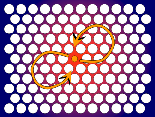
An important and unwanted leakage from a cavity is caused by the fact that light travelling sideways is not reflected back by the mirrors. The unwanted escape could be stopped if one had special mirrors for all three dimensions simultaneously. And this is exactly what the design of the Dutch team employs. Their new design employs three-dimensional photonic crystals as special mirrors, as shown in Figure 1, that reflect certain colors of light in all directions simultaneously. When a point defect is introduced on purpose, the forbidden colors of light are allowed to exist within the photonic band gap crystal. Since such a cavity is completely surrounded by the photonic band gap crystal, the photons cannot escape: they are “locked up in a 3D jail”.
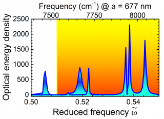
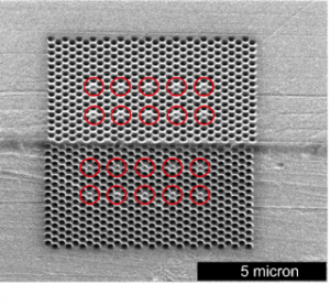
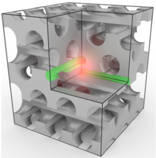
Fabricating a photonic crystal cavity is challenging since it must be made deep inside a 3D structure, a place that is hard to reach. The Twente team employs a diamond-like crystal that is composed of two sets of perpendicular pores, shown in Figure 1. Such crystals have a record-wide band gap, which provides a strong shielding of the cavity. In their design, one pore in each set has a smaller diameter, and at their intersection a point defect appears. Light is then imprisoned in a tiny volume about the defect, as shown in Figure 1. The Twente team studied the enhancement of the energy within the cavity. Lead author Devashish enthuses: “Using elaborate computations on a parallel cluster, we find that the optical energy is remarkably enhanced in the minuscule volume of cavity, by up to 2400´ compared to outside the crystal (see Figure 2). It is really amazing that large enhancements occur even though the structures we studied are razor thin, less than 1.5 microns!” Therefore, the Twente team projects that such cavity structures can readily be integrated in modern high-tech devices, made by CMOS-compatible nanotechnology, see Figure 3.
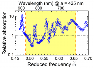
By smartly adapting the periodicity of the crystal, the team found that their photonic band gap cavity reveals a substantial absorption of light in the visible range, up to 10´ compared to bulk silicon (see Figure 2). Group leader Vos quickly points out: “Such a strong absorption in a tiny volume is ideal for sensors. And our devices are 80% lighter than bulk silicon, on account of the many pores in the photonic crystal structure, also referred to as Holeyness.” The Twente study concludes that inverse woodpile cavities offer great potential for optical sensing and photovoltaics.
Previously, the team showed that thin diamond-like photonic crystals reflect a very broad range of colors of light for all angles (http://cops.nano-cops.com/publications/reflectivity-calculated-3d-silicon-photonic-band-gap-crystal-finite-support), which is the basis for the present success. In a concurrent paper in Physical Review B, the team is showing that photons literally “hop” from one cavity to neighboring cavities, thereby revealing unusual “Cartesian” propagation, that is, only in X, Y, or Z directions (completely different from usual light!) The team is confident that intricate photon jails find applications in quantum photonic integrated circuits (PICs) like the recent spin-off Quix (“the fastest way to a quantum future“), see, for instance, www.laserfocusworld.com/articles/2019/01/new-dutch-silicon-nitride-photonics-company-quix-aims-at-quantum-computing.html.
Information not for publication
The team
The research was performed by Dr. Devashish, Dr. Oluwafemi S. Ojambati, Dr. Shakeeb Hasan, Prof. Dr. Jaap van der Vegt, and Prof. Dr. Willem Vos from the Complex Photonic Systems (COPS) chair, and the Mathematics of Computational Science (MACS) chair, both part of the MESA+ Institute for Nanotechnology, at the University of Twente, The Netherlands. Meanwhile Devashish and Hasan have joined ASML the world-leading lithography company, and Ojambati joined Cambridge University (UK) on a prestigious “Rubicon” fellowship. The research project was supported by the Shell-NWO/FOM Program ”Computational Sciences for Energy Research” (CSER).
Further information
For more information please contact: Dr. Devashish, email: d.devashish@utwente.nl, phone: +31-61-632-2202, or: Prof. Dr. Willem Vos, email: w.l.vos@utwente.nl, phone: +31-53-489-5388.
Information on the World Wide Web
The Twente paper is entitled “Three-dimensional photonic band gap cavity with finite support: enhanced energy density and optical absorption” and is being published in the Physical Review B (February 2019), volume 99, article nr. 075112 (Open Access at: https://journals.aps.org/prb/abstract/10.1103/PhysRevB.99.075112).
A pdf of the paper is freely available on the group’s website at https://nano-cops.com/publications/three-dimensional-photonic-band-gap-cavity-finite-support-enhanced-energy-density-and-o as well as on the Cornell preprint server at https://arxiv.org/abs/1808.05607